


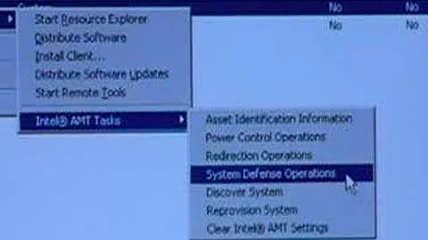
Unlock the Full Potential of MAX 10 ADC Conversion Data with Post-Processing
Find AI Tools No difficulty
No complicated process
Find ai tools
No difficulty
No complicated process
Find ai tools


Are you spending too much time looking for ai tools?
- App rating
- 4.9
- AI Tools
- 100k+
- Trusted Users
- 5000+
 WHY YOU SHOULD CHOOSE TOOLIFY
TOOLIFY is the best ai tool source.
Browse More Content
AI News
- Design services from WhitePage: a creative approach to solving your problems
- Effortless Editing: Object Removal from Photo Techniques
- Tiktok ads spy tool Review
- Monitoring Machine Learning Models with GPU-Enhanced Cloud Services
- 7 Best Weather APIs for AI Tools in 2024
- GeeLark Review 2024
- AI Detector Review: Is it really up to 95% accurate?
- The Safety and Security of Using Trading Bots in Cryptocurrency
- Write Smarter | Top AI Paraphrasing Tools in 2024
- How to understand different types of hosting for your business
GPTS
- Discover Leanbe: Boost Your Customer Engagement and Product Development
- Unlock Your Productivity Potential with LeanBe
- Unleash Your Naval Power! Best Naval Civs in Civilization 5 - Part 7
- Master Algebra: Essential Guide for March SAT Math
- Let God Lead and Watch Your Life Transform | Inspirational Video
- Magewell XI204XE SD/HD Video Capture Card Review
- Discover Nepal's Ultimate Hiking Adventure
- Master the Art of Debugging with Our Step-by-Step Guide
- Maximize Customer Satisfaction with Leanbe's Feedback Tool
- Unleashing the Power of AI: A Closer Look
Stable Video Diffusion
- Transform Your Images with Microsoft's BING and DALL-E 3
- Create Stunning Images with AI for Free!
- Unleash Your Creativity with Microsoft Bing AI Image Creator
- Create Unlimited AI Images for Free!
- Discover the Amazing Microsoft Bing Image Creator
- Create Stunning Images with Microsoft Image Creator
- AI Showdown: Stable Diffusion vs Dall E vs Bing Image Creator
- Create Stunning Images with Free Ai Text to Image Tool
- Unleashing Generative AI: Exploring Opportunities in QE&T
- Create a YouTube Channel with AI: ChatGPT, Bing Image Maker, Canva
Gemini AI
- Google's AI Demo Scandal Sparks Stock Plunge
- Unveiling the Yoga Master: the Life of Tirumalai Krishnamacharya
- Hilarious Encounter: Jimmy's Unforgettable Moment with Robert Irwin
- Google's Incredible Gemini Demo: Unveiling the Future
- Say Goodbye to Under Eye Dark Circles - Simple Makeup Tips
- Discover Your Magical Soul Mate in ASMR Cosplay Role Play
- Boost Kidney Health with these Top Foods
- OpenAI's GEMINI 1.0 Under Scrutiny
- Unveiling the Mind-Blowing Gemini Ultra!
- Shocking AI News: Google's Deception Exposed!
Related Articles

Refresh Articles
