


Intel and UMC Unite for Cutting-Edge Semiconductor Process
Find AI Tools No difficulty
No complicated process
Find ai tools
No difficulty
No complicated process
Find ai tools


Most people like
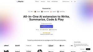
Merlin AI

 1.4M
1.4M
 16.95%
 5
5
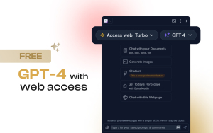
1-click access to AI-powered ChatGPT, GPT-4, Claude2, and Llama 2 for all websites.
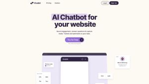
AI Chatbot
Large Language Models (LLMs)
AD
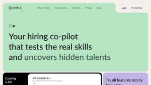
Potis AI
< 5K
 17.89%
4
17.89%
4
Clean and fast bulk candidates screening with behavioral interviews and real case assessments.
AI Interview Assistant
AI Recruiting
AD
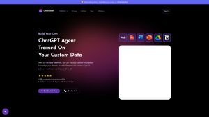
Chaindesk AI
27.1K
9.92%
22
Create custom AI chatbots with Chaindesk for streamlined customer support.
AI Chatbot
Large Language Models (LLMs)
No-Code&Low-Code
AI Product Description Generator
AI Reply Assistant
AI Response Generator
AD

Faircado
15.6K
 66.97%
4
66.97%
4
AI-powered second-hand shopping assistant.
AI Search Engine
AI Product Description Generator
AD

Easy-Peasy.AI
874.9K
22.98%
12
Easy-Peasy.AI is an AI tool that helps users generate original content faster and improve writing skills.
AI Blog Writer
AI Content Generator
AI Creative Writing
Copywriting
General Writing
Writing Assistants
AD
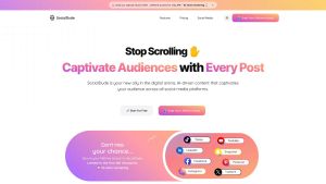
Socialdude.ai
5.5K
 62.75%
7
62.75%
7
AI-driven content creation for all social platforms.
AI Ad Creative Assistant
AI Ad Generator
AI Advertising Assistant
AI Content Generator
AI Instagram Assistant
AI Social Media Assistant
AD
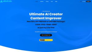
AimindCrafter
< 5K
14
Cutting-edge text creation technology.
General Writing
Text to Image
AI Blog Writer
AI Rewriter
AI Content Generator
AI Creative Writing
Writing Assistants
AI Photo & Image Generator
AI Analytics Assistant
Photo & Image Editor
AI Product Description Generator
Copywriting
Text-to-Speech
Large Language Models (LLMs)
AI Ad Creative Assistant
AI Ad Generator
AI Chatbot
AI Illustration Generator
AI Script Writing
Summarizer
Paraphraser
AI Email Writer
AI Advertising Assistant
AI Poem & Poetry Generator
AI Story Writing
AI Lyrics Generator
Essay Writer
AD
Aili
11.1K
 38.23%
2
38.23%
2
Boost Knowledge Acquisition & Minimize AI Subscription Costs
AI Chatbot
AI Reply Assistant
AI Knowledge Base
Large Language Models (LLMs)
Life Assistant
AD
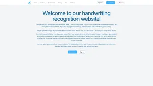
Pen2txt
< 5K
31.34%
4
Effortlessly transform handwritten notes into digital text
Handwriting
Transcription
Transcriber
AD
Wonderchat
61K
31%
3
Create custom chatbot with Wonderchat, boost customer response speed by 100% and reduce workload.
AI Chatbot
AI Reply Assistant
Large Language Models (LLMs)
AD

DreamGen: AI role-play & story-writing
247.3K
26.72%
5
Unleash your imagination with DreamGen.
AI Story Writing
AI Character
Prompt
Large Language Models (LLMs)
AI Creative Writing
AD
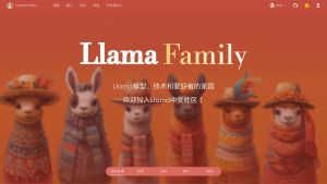
Llama中文社区
14.5K
 62.5%
2
62.5%
2
Home for Llama models, technologies, and enthusiasts.
Large Language Models (LLMs)
AI Knowledge Base
AI Knowledge Graph
AD
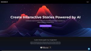
Storynest.ai
170.2K
45.37%
12
StoryNest.ai revolutionizes content creation with AI, providing engaging and informative stories and articles.
AI Story Writing
Writing Assistants
AI Creative Writing
AI Book Writing
AI Content Generator
AD
Are you spending too much time looking for ai tools?
- App rating
- 4.9
- AI Tools
- 100k+
- Trusted Users
- 5000+
 WHY YOU SHOULD CHOOSE TOOLIFY
TOOLIFY is the best ai tool source.
Browse More Content
AI News
- How to boost your SQL Coding Efficiency in a Multi-Database Environment
- Unleash Your Potential: Why ITIL Certification is the Smartest Investment for Your Future
- Navigating the Web Unseen: How Dolphin Anty Shields Your Digital Identity
- Human Writing vs. AI Writing: What to Choose for College Education Needs
- Elevate Your Profits By Leveraging Coinrule's AI Trading Advantage
- A Red Carpet-Worthy Arrival At Dubai’s Most Exclusive Hotels And Resorts With Rented Lamborghini
- Design services from WhitePage: a creative approach to solving your problems
- Effortless Editing: Object Removal from Photo Techniques
- Tiktok ads spy tool Review
- Monitoring Machine Learning Models with GPU-Enhanced Cloud Services
GPTS
- Discover Leanbe: Boost Your Customer Engagement and Product Development
- Unlock Your Productivity Potential with LeanBe
- Unleash Your Naval Power! Best Naval Civs in Civilization 5 - Part 7
- Master Algebra: Essential Guide for March SAT Math
- Let God Lead and Watch Your Life Transform | Inspirational Video
- Magewell XI204XE SD/HD Video Capture Card Review
- Discover Nepal's Ultimate Hiking Adventure
- Master the Art of Debugging with Our Step-by-Step Guide
- Maximize Customer Satisfaction with Leanbe's Feedback Tool
- Unleashing the Power of AI: A Closer Look
Stable Video Diffusion
- Transform Your Images with Microsoft's BING and DALL-E 3
- Create Stunning Images with AI for Free!
- Unleash Your Creativity with Microsoft Bing AI Image Creator
- Create Unlimited AI Images for Free!
- Discover the Amazing Microsoft Bing Image Creator
- Create Stunning Images with Microsoft Image Creator
- AI Showdown: Stable Diffusion vs Dall E vs Bing Image Creator
- Create Stunning Images with Free Ai Text to Image Tool
- Unleashing Generative AI: Exploring Opportunities in QE&T
- Create a YouTube Channel with AI: ChatGPT, Bing Image Maker, Canva
Gemini AI
- Google's AI Demo Scandal Sparks Stock Plunge
- Unveiling the Yoga Master: the Life of Tirumalai Krishnamacharya
- Hilarious Encounter: Jimmy's Unforgettable Moment with Robert Irwin
- Google's Incredible Gemini Demo: Unveiling the Future
- Say Goodbye to Under Eye Dark Circles - Simple Makeup Tips
- Discover Your Magical Soul Mate in ASMR Cosplay Role Play
- Boost Kidney Health with these Top Foods
- OpenAI's GEMINI 1.0 Under Scrutiny
- Unveiling the Mind-Blowing Gemini Ultra!
- Shocking AI News: Google's Deception Exposed!
Related Articles


Refresh Articles
