


Optimize Memory Performance in Intel FPGA Devices: A Comprehensive Guide
Find AI Tools No difficulty
No complicated process
Find ai tools
No difficulty
No complicated process
Find ai tools


Most people like
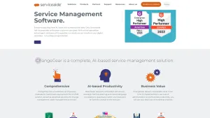
serviceaide.com

 134.6K
 63.43%
 10
10
Modern service management solution for businesses.
AI Customer Service Assistant
AD

Chatbit
10.6K
 13.52%
14
13.52%
14
Custom AI chatbots trained on your data.
AI Chatbot
Writing Assistants
AI Voice Assistants
AD

Chaindesk AI
43.1K
 17.49%
24
17.49%
24
Create custom AI chatbots with Chaindesk for streamlined customer support.
AI Chatbot
Large Language Models (LLMs)
No-Code&Low-Code
AI Product Description Generator
AI Reply Assistant
AI Response Generator
AD

302.AI
< 5K
1
Top AI technologies hub with on-demand payment.
AI Chatbot
Large Language Models (LLMs)
AI Tools Directory
AD
Socratic Lab
7.3K
 47.36%
16
47.36%
16
Collaborative learning and knowledge-sharing platform
AI Analytics Assistant
AI Chatbot
AI Knowledge Base
AI Knowledge Graph
AI Knowledge Management
AD

Merlin AI Plugins
< 5K
13
Merlin: 1-click access to Powerful AI Plugins
AI Chatbot
Large Language Models (LLMs)
Copywriting
Summarizer
Writing Assistants
AI Content Generator
AI Reply Assistant
AI Email Assistant
AI Response Generator
Prompt
AI Social Media Assistant
General Writing
AI Email Writer
AD

Exactly AI
45.7K
16.2%
44
Advanced AI artwork creation platform for artists.
AI Art Generator
Text to Image
AI Photo & Image Generator
AI Illustration Generator
AI Image Enhancer
AI Photo Enhancer
Image to Image
AD

Face Recognition, Liveness Detection, ID Document Recognition SDK
< 5K
 37.79%
9
37.79%
9
Cutting-edge biometric authentication solutions
Large Language Models (LLMs)
AD
Are you spending too much time looking for ai tools?
- App rating
- 4.9
- AI Tools
- 100k+
- Trusted Users
- 5000+
 WHY YOU SHOULD CHOOSE TOOLIFY
TOOLIFY is the best ai tool source.
Browse More Content
AI News
- Navigating the Web Unseen: How Dolphin Anty Shields Your Digital Identity
- Human Writing vs. AI Writing: What to Choose for College Education Needs
- Elevate Your Profits By Leveraging Coinrule's AI Trading Advantage
- A Red Carpet-Worthy Arrival At Dubai’s Most Exclusive Hotels And Resorts With Rented Lamborghini
- Design services from WhitePage: a creative approach to solving your problems
- Effortless Editing: Object Removal from Photo Techniques
- Tiktok ads spy tool Review
- Monitoring Machine Learning Models with GPU-Enhanced Cloud Services
- 7 Best Weather APIs for AI Tools in 2024
- GeeLark Review 2024
GPTS
- Discover Leanbe: Boost Your Customer Engagement and Product Development
- Unlock Your Productivity Potential with LeanBe
- Unleash Your Naval Power! Best Naval Civs in Civilization 5 - Part 7
- Master Algebra: Essential Guide for March SAT Math
- Let God Lead and Watch Your Life Transform | Inspirational Video
- Magewell XI204XE SD/HD Video Capture Card Review
- Discover Nepal's Ultimate Hiking Adventure
- Master the Art of Debugging with Our Step-by-Step Guide
- Maximize Customer Satisfaction with Leanbe's Feedback Tool
- Unleashing the Power of AI: A Closer Look
Stable Video Diffusion
- Transform Your Images with Microsoft's BING and DALL-E 3
- Create Stunning Images with AI for Free!
- Unleash Your Creativity with Microsoft Bing AI Image Creator
- Create Unlimited AI Images for Free!
- Discover the Amazing Microsoft Bing Image Creator
- Create Stunning Images with Microsoft Image Creator
- AI Showdown: Stable Diffusion vs Dall E vs Bing Image Creator
- Create Stunning Images with Free Ai Text to Image Tool
- Unleashing Generative AI: Exploring Opportunities in QE&T
- Create a YouTube Channel with AI: ChatGPT, Bing Image Maker, Canva
Gemini AI
- Google's AI Demo Scandal Sparks Stock Plunge
- Unveiling the Yoga Master: the Life of Tirumalai Krishnamacharya
- Hilarious Encounter: Jimmy's Unforgettable Moment with Robert Irwin
- Google's Incredible Gemini Demo: Unveiling the Future
- Say Goodbye to Under Eye Dark Circles - Simple Makeup Tips
- Discover Your Magical Soul Mate in ASMR Cosplay Role Play
- Boost Kidney Health with these Top Foods
- OpenAI's GEMINI 1.0 Under Scrutiny
- Unveiling the Mind-Blowing Gemini Ultra!
- Shocking AI News: Google's Deception Exposed!
Related Articles


Refresh Articles
